
Materials Science for Photonics Applications
Single Crystal Metal Growth for Plasmonics and Electronics
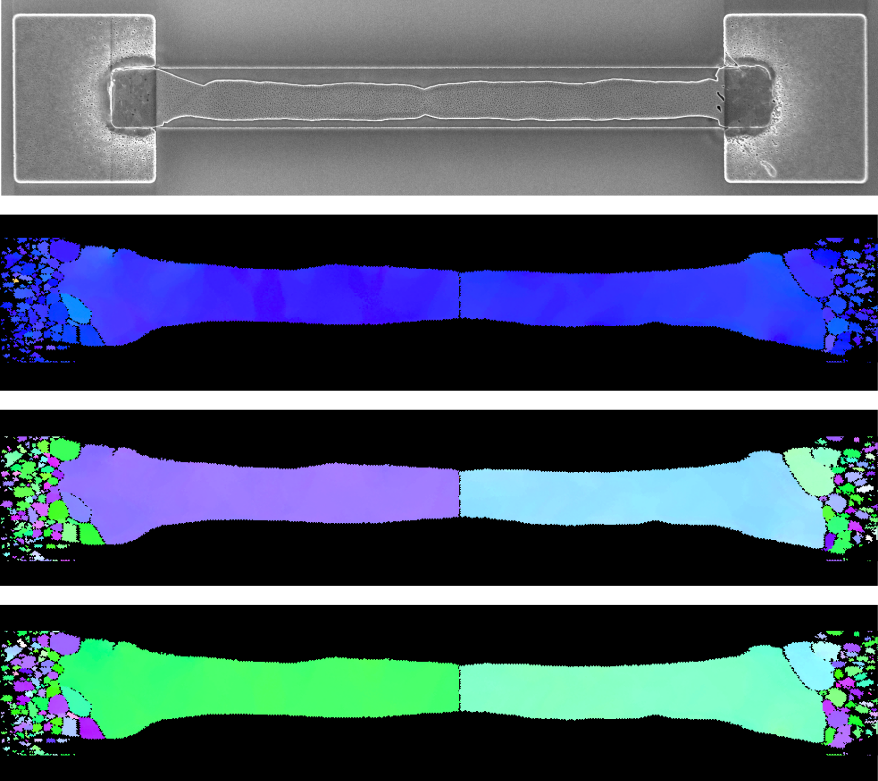
The mechanical, thermal, optical, and electrical properties of metals are specified by their crystallinity and microstructure. In the nano-scale regime, single crystalline metals are stronger, exhibit lower electrical resistivities, exhibit lower plasmonic losses, and are more resistant to electromigration over their polycrystalline counterparts. These more favorable attributes have motivated the scientific community into developing new ways of fabricating single crystal metal devices. We have developed a new technique, based on rapid-melt growth and liquid phase epitaxy, which produces single crystal gold microstructures on amorphous insulating substrates. These structures can be further patterned with lithography into functional devices and is largely scalable. We envision that this materials platform will enable new scientific study into fundamental metallurgical properties and will serve as a core technological process in advanced plasmonic and electronic systems.
Materials for Visible Light Metasurfaces
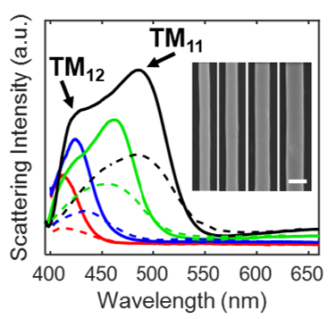
A major challenge to scaling metasurfaces to the visible spectrum is identifying and processing high contrast, transparent thin films. Current candidate materials, such as silicon nitride, titanium dioxide, and gallium nitride, are fully transparent but provide limited dielectric contrast. We have identified single crystal silicon as a viable, high contrast material for fabricating metasurfaces across the visible regime. Our analysis indicates that while bulk single crystal silicon is not transparent at visible wavelengths, the absorption losses of single crystal silicon are sufficiently small such that thin films of the material are effectively or nearly transparent at these wavelengths. We experimentally characterize resonators and metasurfaces made from single crystal silicon by bonding SOI wafers to Pyrex wafers, followed by backside polishing and patterning. Devices designed for wavelengths as short as 488nm exhibit high efficiencies.
Metal Oxide Materials
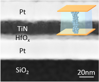
Metal oxides are versatile materials used broadly in electronic, photonic, and chemistry applications. We have been exploring the use of soft-breakdown in metal oxide thin films, which can be placed as a spacer between two plasmonic antennas and serve as a mechanism to program antenna optical response. We envision that these concepts can leverage the scalability of devices utilizing soft breakdown, such as RRAM, to produce large area programmable optical materials. We have also been exploring the redox and defect properties of iron oxide particles and films, using a combination of atomistic simulations and experimental materials characterization. Iron oxide is an earth abundant semiconductor used in solar technologies and chemical looping energy conversion applications.