
Dielectric Metamaterials and Metasurfaces
Metasurfaces are diffractive optical components consisting of a layer of subwavelength-scale metal or dielectric structures. Our group is actively researching how to achieve high efficiencies and new functionalities in freeform metasurface systems through the utilization of new nanoscale light-matter interactions. An overview of some of our group’s work on the topic can be found in this article.
Diffractive Gratings with Periodic Metasurfaces
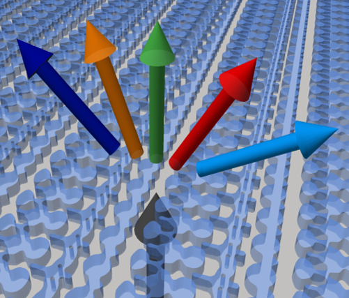
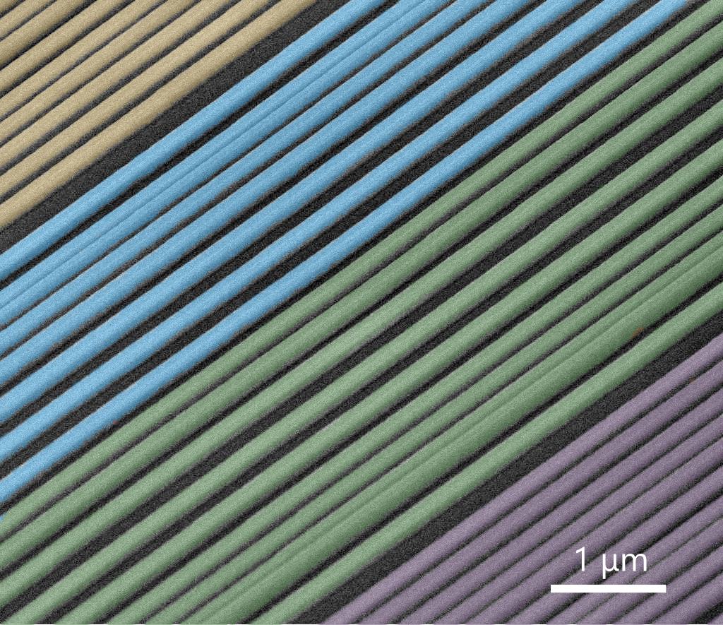
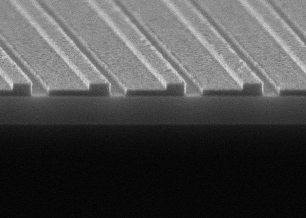
Metasurfaces conventionally consist of simple, physically intuitive shapes, ranging from cylindrical and elliptical posts to rectangular slabs. While devices designed in this manner suggest the promise of nanoscale engineering in diffractive optics application, they do not take advantage of the much vaster phase space for design made accessible by non-intuitive shapes. We use adjoint-based topology optimization to design high performance metagratings, which are periodic metasurfaces that deflect electromagnetic waves to specific diffraction orders. With this technique, we have demonstrated silicon-based near-infrared devices that can efficiently deflect unpolarized light to large angles (70 degrees+), perform wavelength-multiplexed beam splitting, and enable large-angle negative diffraction. The final devices comprise non-intuitive curvilinear shapes and they utilize inter- and intra-mode coupling to achieve high performance.
Topology-Optimized Aperiodic Metasurfaces
The extension of adjoint-based topology optimization to large area, aperiodic phase profiles will enable the realization of high performance optical elements, such as high efficiency, aberration-corrected lenses. However, the direct optimization of such phase profiles presents an immense computational challenge. We propose methods to make these problems more computationally tractable, by sub-dividing the desired phase profiles to small areas, optimizing these sections individually, and then stitching them together. We demonstrate large numerical aperture lenses designed with this technique, which exhibit higher efficiencies than those based on conventional optical phased array elements.
Multi-layer Metamaterials
Metasurfaces today typically consist of a single layer of nanostructures. While much can be achieved with a single layer of nanostructures, there are fundamental limits to their optical responses. We propose to break these limits by extending the design of metasurfaces to multi-layer metamaterials. By using topology optimization to simultaneously design multiple closely-interacting layers in a metamaterial, we can access and exploit significantly more design degrees of freedom to produce high efficiency, aberration-corrected optical elements. We can also extend the functionality of this thin-film platform to other classes of optical devices, such as filters.